Article posted on Dec 29, 2016
Solder bumps are used to connect die to various package components in advanced packaging processes. Bump height and coplanarity are critical to ensuring reliable connections. A bump that is not high enough will not connect, while one that is too tall may prevent connection by neighboring bumps or even damage an electrical tester’s probing card. Measuring true bump height quickly and accurately has proven to be a challenge.
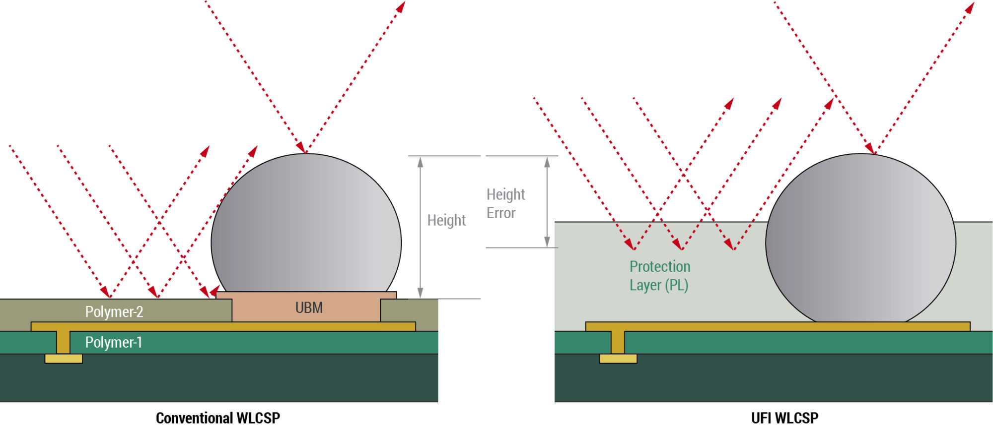
The measurement has become more challenging with the introduction of processes that eliminate the under bump metal (UBM) layer, used in conventional wafer-level chip scale packages (WLCSP) to improve the bond between the solder ball and the copper redirect pad. Wafer-level chip scale packages have been limited in chip size and ball pitch by the fragility of the solder ball-redirect connection. The intermetallic compounds (IMC) formed there are mechanically weak and subject to fracture under the thermally induced mechanical stress generated by the different expansion coefficients of the silicon die and the package substrate. In UBM-free integration (UFI), the UBM is eliminated and the solder connects directly to the redirect pad. A thick polymer protection layer (PL), usually polyimide (PI) or polybenzoxazole (PBO), helps secure the solder in place and provides stress relief between the chip and the substrate. In addition to eliminating the IMC as a source of failure, UFI reduces package cost and cycle time by eliminating layers, and allows a significant reduction in final package thickness. Unfortunately, the PL layer, which is semitransparent and varies in thickness, introduces errors in bump height measurements.